
Software / PCB 3D Builder
PCB 3D Builder
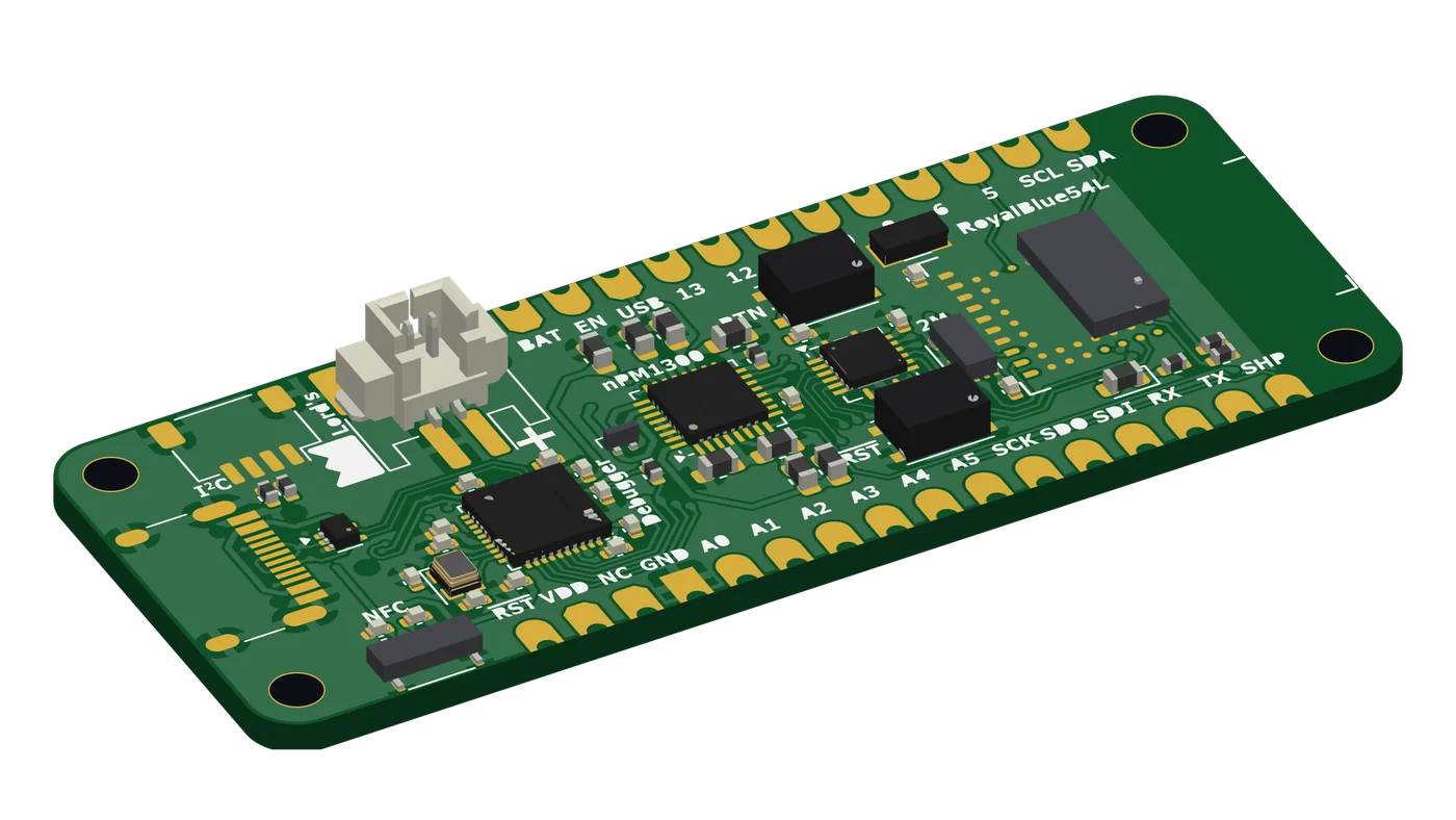
Your design files, in 3D with every part.
ASC · Gerber + placement · DXF — whatever CAD they came from, just drag the files in.
Part 3D models are found in the KiCad library and fitted automatically, then saved as STEP for mechanical design.
01 / Why it matters
More dimension.
Less manual work.
If you have PCB design data but no 3D model with the parts placed, working with mechanical design may mean ordering separate modeling or doing extra work yourself.
No 3D model yet
Design data alone gives mechanical design no 3D model to work with, so separate modeling or extra work may be needed.
Finding and fitting every part
Finding a 3D model for each part, then placing and orienting them one by one, takes time and effort.
From design data to STEP
PCB 3D Builder uses your design data and parts library to help build the model, check and adjust it, and hand it over as STEP. It helps reduce the time and cost of separate modeling.
The model is reference material for design review; mechanical design and a final review are still needed.
02 / Quick Guide
Drop in, check.
Save as STEP.
Six steps from Gerber, PADS ASC or DXF to a PCB 3D model (STEP file), shown with real screens of the program (4.0). Click a picture to enlarge it. The program interface is in Korean.
What to put in
- Most accurateASC
A single PADS ASCII file gives the outline, parts, pads, silkscreen and traces.
- Without ASCGerber + placement
Just the Gerbers and placement file everyone gets for PCB orders and SMT. The placement file can be Excel, CSV or TXT.
- Without GerbersDXF + placement
A mechanical DXF and a placement file give the board and part placement.
Placement files it reads
SMT placement files (pick & place · centroid · component locations) differ by CAD, but column names and separators are recognized from the content. No need to rename files or convert them to Excel.
| Format | Extension | Examples |
|---|---|---|
| Excel | .xlsx.xls | Placement data from SMT houses and vendors |
| CSV | .csv.txt | Altium Pick and Place · KiCad · OrCAD/Allegro · PADS export |
| Text report | .txt | P-CAD Component Locations · Altium Pick and Place (text) |
| Space-separated text | .txt.pos | KiCad .pos · Allegro place_txt |
| Eagle mount file | .mnt.mnb | Eagle (no header line) |
Only reference, X and Y are required; rotation, side, footprint and value are used when present. Units (mm/mil), origin and Y direction are matched to the Gerbers automatically.
PCB 3D in six steps
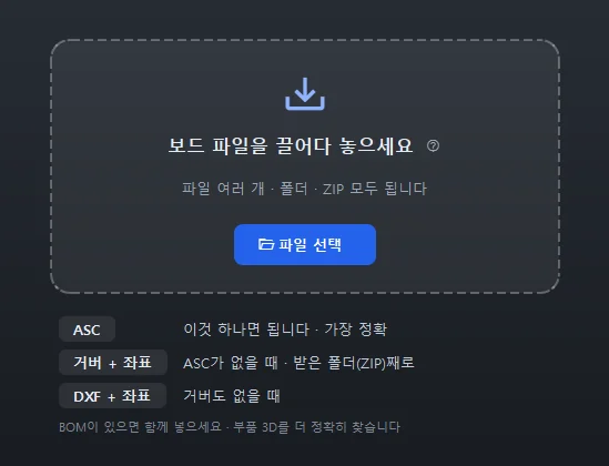
- 01
Drop in the files
Drop the whole delivery folder or ZIP from your vendor. ASC, Gerber, placement and BOM files are told apart by their content.
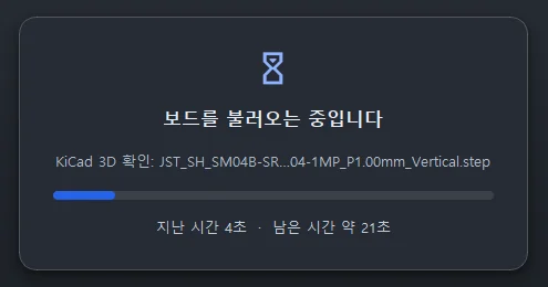
- 02
Read and matched automatically
Outline, drills and pads are read, and the origin, Y axis, units and rotation rules are matched automatically, with the current task and time left shown.
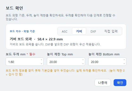
- 03
Check the board
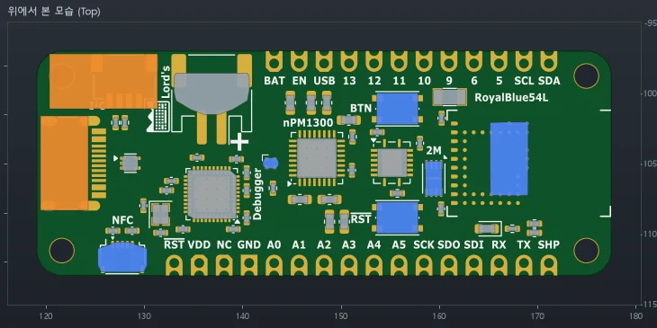
Just confirm the outline reference, board thickness and enclosure height limit. Parts taller than the limit are outlined in red.
- 04
Fill in part 3D automatically
Real models are found in the KiCad 3D library and fitted to the pads; without a match, the package is built from its dimensions. Parts that are not packages, such as connectors, need a STEP file.
- 05
Check and adjust
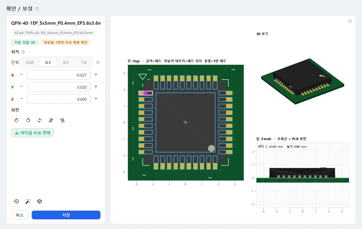
Overlay the 3D model and the pads to confirm pin 1 and polarity, and fix them in a few clicks if needed. On Gerber boards pin 1 is estimated from the silkscreen, so do check it.
- 06
Save as STEP
Save a STEP ready for your mechanical CAD, with silkscreen, copper and part names. You can keep working while it saves.
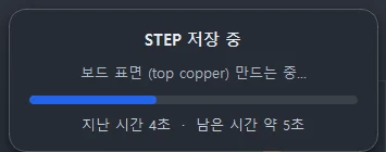
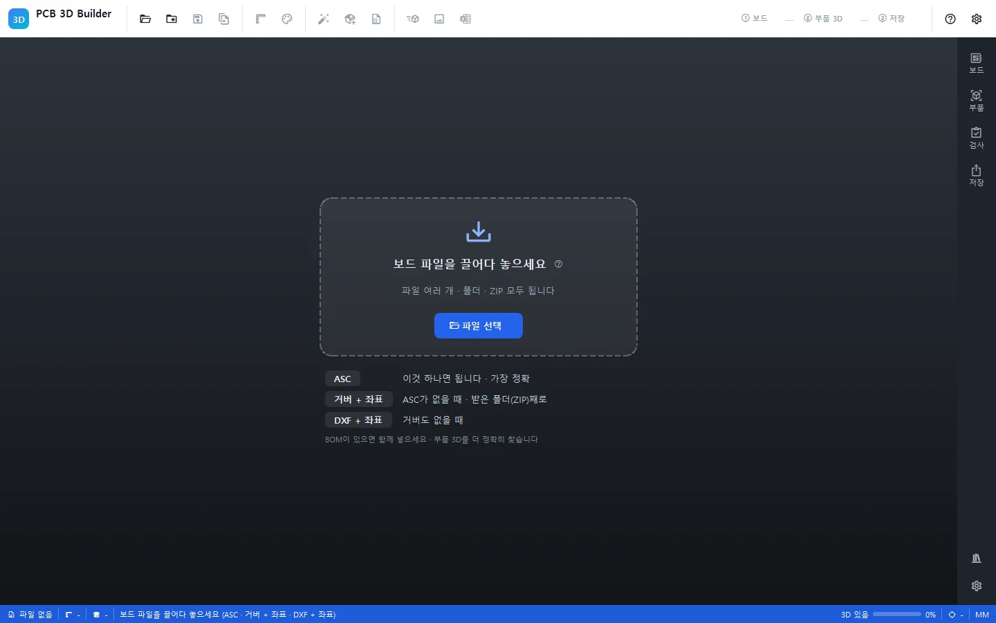
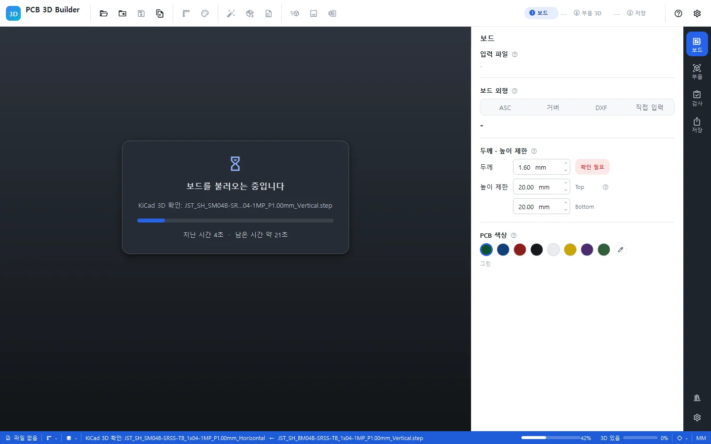
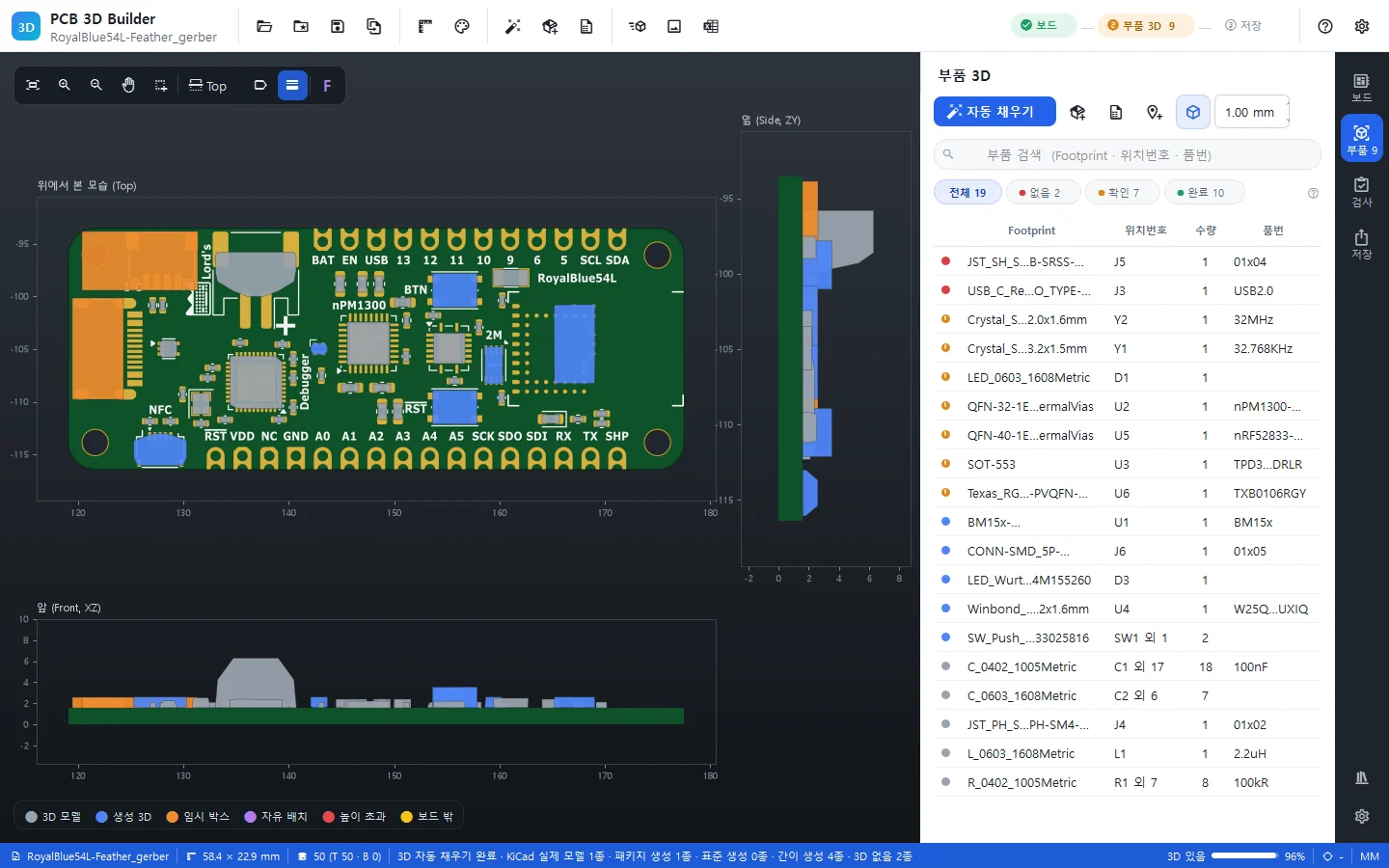
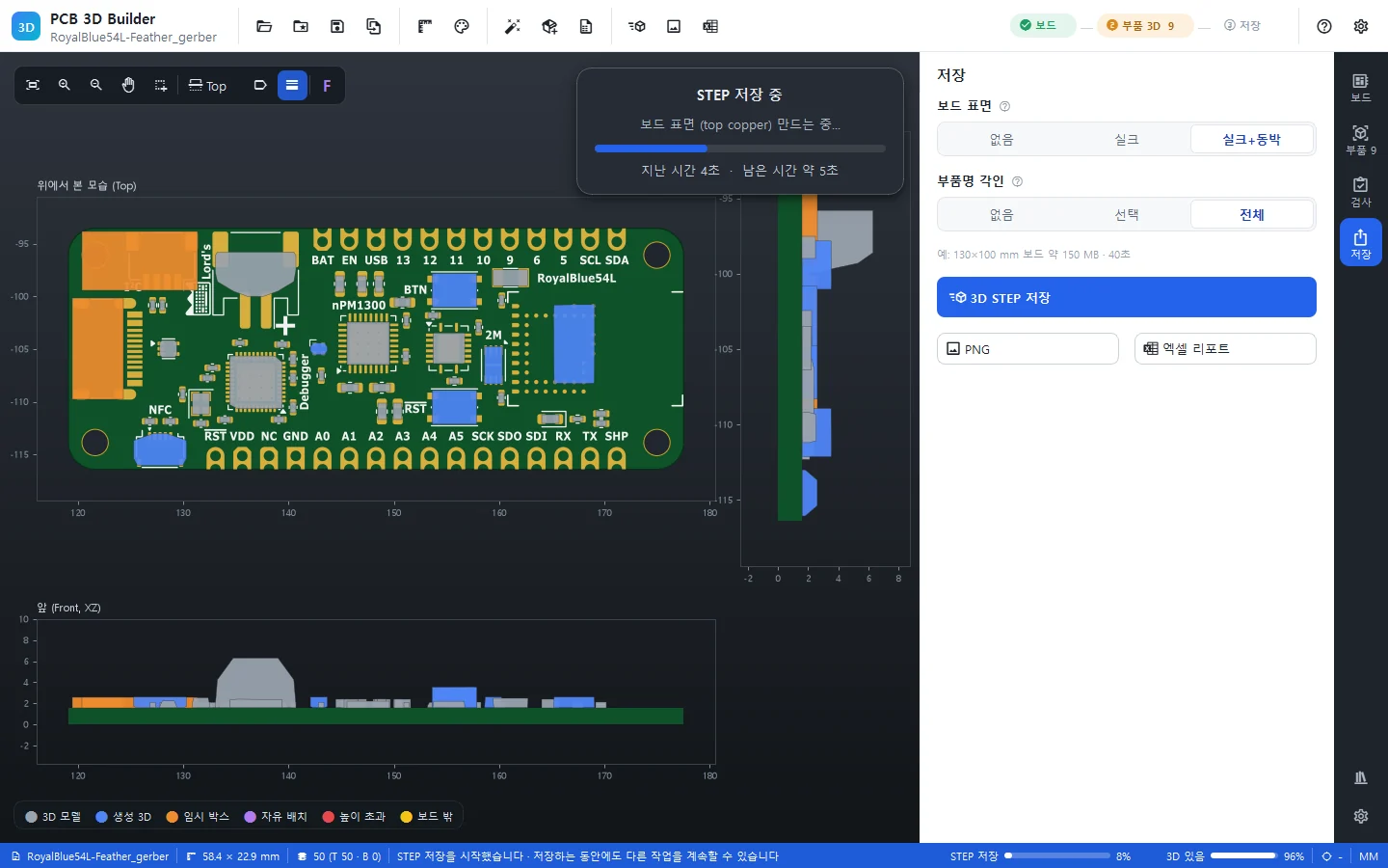
Each step is explained in detail in the user guide. Example board on screen: KiCad example ‘RoyalBlue54L Feather’ (CERN-OHL-P v2)
03 / Features
Models filled in.
Less work by hand.
Model Matching
Model matching · auto alignment
[3D auto-fill] fills parts with real KiCad models, then generated packages, then standard chip shapes, then simple pad-based models. KiCad models are found by footprint, part number, package code, online part data and pad layout, even when the name has no package in it. With ASC input, IC pin 1 and diode polarity are aligned too.
Package Generation
Automatic package generation
Parts with no KiCad model are built from a package dictionary (SOIC · SSOP · TSSOP · SOT · QFN · DFN · LQFP · SOD · SMA/SMB/SMC · PowerPAK · electrolytic capacitors · power inductors · crystals/oscillators and more): the package that fits the pads is chosen and leads are placed on the pads.
Check & Adjust
Part check & adjust
Double-click a part to compare its 3D model with the pads, pin 1 pad and board top surface, then rotate it by 90° or 180°, enter coordinates, drag it, or drop it onto the board surface. Adjustments are saved per footprint in the library and reused on the next board.
Per Reference
Per-reference settings
Give one part its own 3D or adjustment, or remove it from the 3D, while other parts with the same footprint stay as they are. Useful when the same footprint sits on the top and bottom at the same spot and the 3D appears twice. The ASC file is not changed.
Free Placement
3D free placement
Place parts that are not in the ASC (STEP · ZIP) anywhere on the board to check a concept or clearance, for example a sub board mounted on the main board. They are included in the height and outside-board checks and in the STEP.
Board Preview
Board preview
Top, front and side views are shown together; switch between top and bottom (mirrored). Release an area zoom with ESC or a single click, and click a part to see its reference, height and side.
Gerber Input
Boards from Gerber + placement files
No ASC needed: the Gerbers you send for PCB orders and the SMT placement file are enough, from any CAD. Copper, exposed pads and silkscreen go in exactly as in the Gerbers. Drop a whole folder or ZIP and the Gerbers, placement file and BOM are found.
STEP Options
Board surface · color · labels
With ASC input, the STEP can include silkscreen, copper and traces. Choose the PCB color and whether to engrave part names (none · selected · all).
Height & Report
Height check · review report
Enter the enclosure’s inner height to outline taller parts in red; parts outside the board are outlined in yellow. The Excel report lists placement, parts without 3D, height overruns and parts outside the board, gathering what to check after the model is built.
04 / Use Cases
See it in 3D.
Plan the next design.
Examples based on the features, not actual customer cases. The 3D models, STEP files and reports are reference material for design review; check them yourself before using them for mechanical design, manufacturing or production.
Example 01 / Mechanical
STEP for enclosure design review
Create a PCB 3D STEP with the board outline, mounting holes and part placement for enclosure and mechanical design review. Add a sub board or extra parts with 3D free placement to check the assembly.
Example 02 / Clearance
Checking enclosure height clearance
Find parts that exceed the enclosure's inner height in advance and list them in the placement report.
Example 03 / Library
Building a team parts library
Parts you fill in and adjust with STEP · ZIP files are saved to the library folder; point it to a NAS or shared folder so the team can reuse them on the next board.
Cases
Cases
05 / Specifications
What you start with.
What you end up with.
| Reference version | PCB 3D Builder 4.0 (per the user manual) |
|---|---|
| Board input | Start from one of these. PADS ASCII (.asc, recommended): PowerPCB V4 to the latest version (coordinate units BASIC · MILS · METRIC · INCHES). Reads the board outline, mounting holes, part placement, pads, silkscreen, traces and copper; without a board outline, an outline is estimated from drawing lines. Gerber + placement file: Gerbers (folder · ZIP) from any CAD plus the SMT placement file. Outline, mounting holes, pads, copper and silkscreen come exactly from the Gerbers; origin, units and bottom rotation are matched automatically to the Gerber pads. Without pin numbers, IC pin 1 and polarity are estimated from the silkscreen. DXF (top · bottom): a PADS DXF carries reference designators, footprints, rotation and side and works on its own; a mechanical CAD DXF needs a placement file (Excel · CSV). With DXF, the STEP contains the board and parts without silkscreen or copper. The board outline reference can also be entered manually (width · height · corners · mounting holes). |
| Part information | BOM (bill of materials, Excel · CSV) — optional. Improves finding part models by part number. |
| Part 3D | Library models · KiCad 3D models · your STEP / STP / ZIP files · standard chip shapes (0402–2512) · generated packages · simple pad-based models · temporary boxes. The dot color in the parts list (red · orange · blue · gray) shows each part’s status. |
| Generated packages | SOIC · SOP · SSOP · QSOP · TSSOP · MSOP · SOT · SC-70 · PowerSSO · HSOP · QFN · DFN · LQFP · TQFP · SOD · SMA/SMB/SMC · PowerPAK · electrolytic capacitors · power inductors · crystals/oscillators · chip arrays. Used when no KiCad model exists; the package that fits the pads is chosen. Parts that are not packages, such as connectors and switches, need a STEP file. |
| Output | 3D STEP — the 3D model for mechanical design (main output) Extras: preview PNG (image export) · placement report in Excel (placement list, no 3D, height overruns, outside the board) Save your work as a project file (.p3d) to continue later. |
| Board preview | Top, front and side views together (default), top / bottom switch (mirrored), area zoom (release with ESC or a single click), part reference, height and side on click |
| Part check & adjust | Double-click a part to compare it with the pads (gold), pin 1 pad (pink) and board top surface (green line). Rotate Z ±90° · 180° · X/Y 90°, enter coordinates or drag, drop onto the board surface. One part of a shared footprint can be set on its own (per-reference settings) |
| Operating system | Windows 10 / 11, 64-bit |
| Internet use | Board files and design data are never sent out. The internet is used to download KiCad 3D models (gitlab.com, raw.githubusercontent.com), to open a web browser from [온라인 검색] (Online search), and for the online part check when it is on (only part numbers go to the JLCPCB/LCSC part search; it can be turned off in Settings). On a PC with KiCad installed, the models in its install folder are used. |
| Installation | One installer (Setup.exe). Can also be installed for the current user only, without administrator rights. Installing over an earlier version keeps the parts library, settings and project files. |
| License | Free of charge for personal and business (commercial) use. The original installer may be passed on to others only unmodified and free of charge. Provided “as is” without warranty. The license agreement shown during installation applies. |
06 / FAQ
Questions before you start.
Answered one by one.
01Which design files do I need?
A single PADS ASCII (.asc) file is recommended. Without ASC, use the Gerbers from your PCB order with the SMT placement file, or DXF (top · bottom) with a placement file (Excel · CSV) if needed. A BOM and part STEP · ZIP files are optional extras that help.
02I design in a CAD other than PADS. Can I use it?
Yes. From 4.0, any CAD — Altium, OrCAD/Allegro, KiCad, Eagle, P-CAD and more — works with the Gerbers from your PCB order and the SMT placement file, and copper and silkscreen go into the STEP exactly as in the Gerbers. Gerbers have no pin numbers, so IC pin 1 and diode polarity are estimated from the silkscreen; check parts marked “pin 1 check”. DXF with a placement file also works, but then the STEP has the board and parts without silkscreen or copper.
03Is a BOM required?
No, it is optional. It improves finding part model candidates by part number.
04Are all parts built accurately and automatically?
No. 3D auto-fill uses real KiCad models, then generated packages, then standard chip shapes, then simple pad-based models and aligns them to the pads, but some parts may remain without 3D or need a check. These are mostly parts such as connectors and switches that need a STEP file. Drag a STEP from [온라인 검색] (Online search) onto the part’s row, or adjust it in the check & adjust view. Parts you do not need can also be removed (saved per board, restorable any time).
05I was using an earlier version. How do I update?
Run the new installer without removing the old version; it installs over it. The parts library (Documents\PCB3D_Library), settings and project files are kept. Coming from 2.x, open an ASC and run [3D auto-fill] once: parts created automatically before are searched again with the new rules, while parts you assigned or adjusted stay as they are. “3D from PDF” was removed in 3.0.
06Which output formats can I save?
3D STEP (model for mechanical design collaboration), preview PNG (image for review and sharing) and the Excel placement report (placement list plus no-3D, height-overrun and outside-board items). Work in progress is saved as a project file (.p3d). The outputs are reference material for design review; compare them with the original design before manufacturing.
07Can I use it without the internet?
Board files are processed on your PC, and board files and design data are never sent out. The internet is needed to download new KiCad models, for [온라인 검색] (Online search), and for the online part check (only part numbers are sent; it can be turned off in Settings). Behind a company firewall, allow gitlab.com · raw.githubusercontent.com · jlcpcb.com or install KiCad on the PC.
08Is it free for company use?
Yes. Under the license agreement it is free of charge for both personal and business (commercial) use. You may not sell it or distribute modified versions, and the original installer may be passed on only unmodified and free of charge. The program is provided “as is”.
09How do I download it?
Leave a question or a short note on how you plan to use it, and we will email you a one-time download code. The code works once within 10 minutes; the button in the email opens the download page with the code filled in. If the email does not arrive, press "Send the code again" or check your spam folder.
10Windows shows a “Windows protected your PC” warning.
This is a normal warning for a program without a code signature. Click [More info] in the blue window first, then [Run anyway]. If there is no [Run anyway] button or a company PC blocks it, see If installation is blocked below the download.
11Why do you ask for an email and company name?
To issue the download code and to answer your message. They are kept for one year and then deleted automatically, or immediately on request. They are never shown in the Q&A.
12Will the STEP file open in mechanical CAD such as SolidWorks?
Yes. STEP is the standard 3D format mechanical CAD tools share, so SolidWorks, Creo, Inventor, Fusion 360 and similar tools can import it. The board outline, mounting holes and part heights are included, ready for enclosure design and clearance checks.
13Do I need to find part 3D models (STEP) myself?
Mostly not. Real models are found in the KiCad 3D library automatically, and packages are built from their dimensions when none exists. Only non-package parts such as connectors and switches need a STEP or ZIP from the maker or an online search; once added, the 3D is saved in the library and reused on the next board.
07 / Download
Getting ready for your next STEP.
Download coming soon
- 01Leave a question or use case
- 02Get a one-time code by email
- 03Download with the code (once, within 10 minutes)
- Version
- Operating system
- Windows 10 · 11 (64-bit)
- File size
- License
- Free for personal and business use. No selling or modified redistribution; the original installer may be passed on free of charge. Provided as is.
Check your email
We sent an 8-character download code to .
The code works once, for 10 minutes (time left 10:00). The button in the email opens this page with the code filled in. If you cannot find the email, check your spam folder.
If installation is blocked When “Windows protected your PC” appears or setup does not start
PCB 3D Builder has no code signature, so Windows asks for confirmation with a blue window the first time it runs. This is a normal warning, not a problem with the program. Only use an installer downloaded from this page.
When the blue “Windows protected your PC” window appears
- Click the [More info] link in the blue window.
- The window changes to show “App: PCB3D_Builder_Setup_….exe” and “Publisher: Unknown publisher”, and a [Run anyway] button appears below.
- Click [Run anyway] to start the installation.
[Don’t run] simply closes the window. Always click [More info] first.
When there is no [Run anyway] button after [More info]
The company PC blocks it with a security policy.
- Option 1: right-click the downloaded exe → [Properties] → check “Security: Unblock” at the bottom → [OK], then run it again.
- Option 2: if it still does not run, ask that PC’s IT administrator to allow it. Users cannot change this setting themselves.
Other blocks
- The browser blocks the download: if Edge or Chrome says the file “isn’t commonly downloaded” and does not keep it, open the file’s menu (…) in the download list and choose [Keep].
- Antivirus removes the file: restore it from quarantine or add an exception. If the antivirus is managed by your company, ask your IT administrator.
- No administrator rights: choose “Install for current user only” as the installation scope.
Before installing, see the user guide for the files you need and the workflow.
Updates
Next versions.
Next possibilities.
PCB 3D Builder keeps improving in features and usability.
What changed in 4.0 — boards from Gerber + placement files (any CAD), the board surface exactly as in the Gerbers (copper · exposed pads · silkscreen), a start screen for dropping files, folders and ZIPs, a progress card with estimated time left, removing parts without 3D, a 20 mm default height limit, the board check window on every open, and faster preview and STEP export for large boards.
From Knowledge to Product
Beyond the model.
Into the product, together.
Start by telling us your current challenge and the features you need.